Let’s recap for a minute the progress of the voltage regulator circuit board.
I started out with a proof-of-concept “bread board” circuitry, on which I tested the validity of the idea.
 |
| Original proof-of-concept board |
Later, I conducted full power tests on the heating element using components mounted on a blank board.
 |
| Full power testing board |
Now, I will take you through the process of making the actual circuit board. This board will reside inside an enclosure, and supply metered power to the heated probe.
 |
| Final(ish) design |
There are a number of computer programs that can help with designing a printed circuit board (PCB), in reality they are not really necessary, but they are nice to have to help narrow down the final design.
Right below are some of the programs I checked out. I will not say which one I used, you can pick whichever you like best, or find a better one online.
Express PCB (Windows)
Eagle PCB Software (Windows)
Fritzing (Windows, Mac and Linux)
My design for a voltage regulator has a high setting, and a low setting, selectable via a switch (for now). It is meant to be used in ground mode (low heat), and flight mode (high heat). These values should be pretty close to the final ones, but more testing on Wade’s Pitot will have to confirm them.
 |
| My board design |
In the early ‘80s I used to make my own circuit boards by rubbing the back side of transferable patterns onto copper boards. These were later dipped in acid to dissolve the uncovered copper, leaving only the desired traces.
Today’s methods are still basically the same, but the quality of the final board can be greatly improved by enlisting the help of photographic style processing. Like in the old days, it can still be done at home as I will try to demonstrate.
Back to the PCB design, it is necessary to finalize the design, be it computer based or hand drawn, before proceeding to the next step.
Out of the various methods out there, I chose to use a copper board coated with a substance called “photo resist”. I’m not exactly sure what it’s made of, but whatever it is, the important thing is that it is sensitive to light, and I will use this property to transfer my design onto the board.
I ordered a pre-made kit from www.jameco.com (item #2113244). This kit contains two circuit board with photo-resist on them, one big bottle of ferric chloride, and one little bottle of board developer solution.
 |
| Board creating essentials |
Now, all of these liquids are really really BAD things to get in contact with, as an even cursory reading of their spec sheets will show, so a high level of protection and ventilation is a must.
The steps to the process are:
- Print the circuit on a transparency
- Lay it on the photo resist side of the copper board
- Expose it to bright light for 8 to 10 minutes
- Develop the circuit image onto the board by dipping it in a 1 to 10 solution of developer and water
- Rinse the board in cold water
- Immerse the bard in a 1 to 1 solution of ferric chloride and water for 20 to 30 minutes
- Rinse the board in cold water
- Remove any trace of photo resist with nail polish remover
- Drill the holes for the components
Done!
 |
| Transparency printed at the FedEx store for $0.45 |
 |
Transparency trimmed and laid on a picture frame $2.00
|
 |
| Using an halogen lamp to expose the photo resist on the copper board |
 |
I used clear tape to secure the transparency to the board at the corners
|
 |
You can see the circuit developing on the PCB
|
I should have probably used a regular light bulb, or leave the board in the light longer, because a part of the circuit vanished from the board during development, and other parts were a bit thin.
 |
Circuit fully developed (sort of)
|
I corrected that with a few strokes of permanent marker.
 |
Black marker used to rebuild some of the traces
|
 |
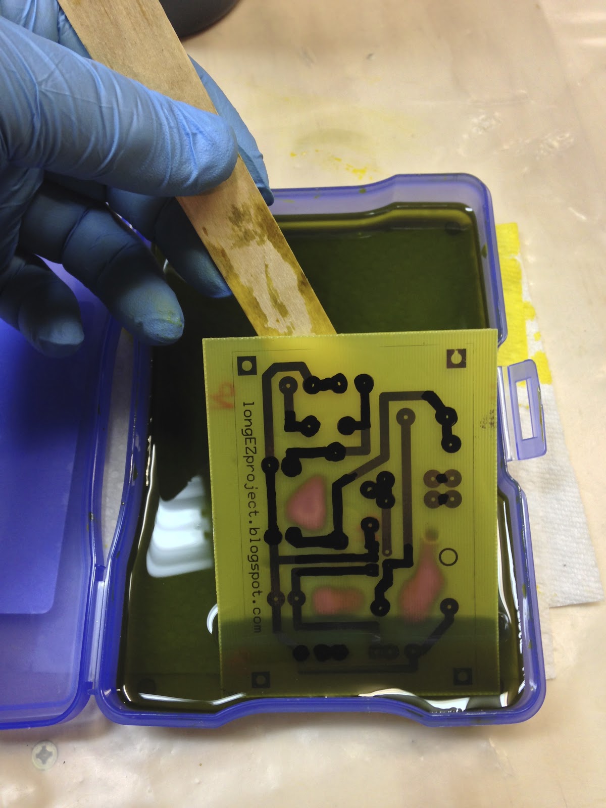
| PCB bathing in ferric chloride |
 |
Ferric chloride eating away the copper from the board
|
 |
Process almost complete
|
 |
Etching process complete
|
 |
| PCB done! Photo resist and black marker removed with nail polish remover. |
 |
PCB nearly ready to go to work
|
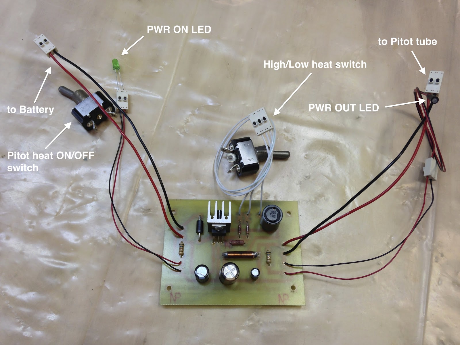 |
finished PCB ready for testing
|
I think I might "massage" the design a bit to produce a smaller PCB, there seems to be a lot of wasted space on the board, but overall I am satisfied with the final product.
I will be looking for a suitable enclosure next, and the final size of the PCB might depend on what box I can find to house it. A smaller PCB is better to a degree, but larger one is easier for me to solder.
I will be looking for a suitable enclosure next, and the final size of the PCB might depend on what box I can find to house it. A smaller PCB is better to a degree, but larger one is easier for me to solder.
No comments:
Post a Comment